Browse categories
English
$
USD
Connect to your AI
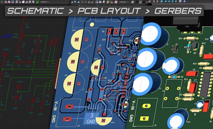
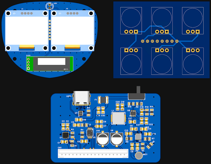
Need your schematic turned into a professional PCB layout?
I will convert your schematic into a high-quality, production-ready PCB layout using KiCad or EasyEDA.
What I can provide:
What you need to provide:
Important: This gig is for PCB layout from an existing schematic. I am not designing or modifying the underlying circuit unless separately agreed.
I will keep the PCB organized and practical for manufacturing while following the requirements you provide.
Please provide complete and clear project information when ordering.


Specialization:
Circuit design
•
Schematics
•
Layout
•
Footprint
•
Gerber
File format:
Gerber
•
SCH
•
Software:
EasyEDA
•
KiCad
Interface:
TDM
•
USB
•
I2C
•
Wi-Fi
•
BLE
•
BT
•
NB-IoT
•
Ethernet
Can you design a PCB from my idea without a schematic?
This gig is specifically for converting an existing schematic into a PCB layout. If you only have an idea or circuit requirements, please contact me first so I can determine whether I can help with the project.
What files will I receive?
Depending on the selected package, you will receive the KiCad project/source files and manufacturing-ready Gerber files. The exact deliverables are listed in each package.
Can you use my preferred components or footprints?
Yes. Please provide the required part numbers, datasheets, or existing footprints when specific components must be used. Otherwise, I will select an appropriate footprint based on the information provided.
Do you manufacture or assemble the PCB?
No. This gig provides the PCB design files and manufacturing files. PCB fabrication and component assembly are not included unless specifically agreed as an additional service.
Can you make changes after the PCB is completed?
Yes. Revisions are included according to the selected package. Revisions cover changes related to the original requirements. Major changes to the schematic, board requirements, or project scope may require an additional charge.
Can you design high-speed, RF, or very complex PCBs?
Please contact me before ordering for high-speed, RF, impedance-controlled, or otherwise highly specialized PCB requirements. I can review the requirements and confirm whether the project is suitable for this gig.