Browse categories
Explore
Fiverr Pro
English
$
USD
PCB Design Engineer IoT, RF, BMS and Industrial Systems
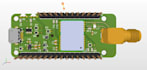
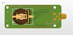
I deslgn high-performance RF PCB layouts for wireless systems including WiFi, Bluetooth (BLE), GSM, GPS, LTE, CAT-M1, NB-IoT, Zigbee, NFC, and RFID, with strong focus on signal integrity, controlled impedance, and low EMI/EMC. Each deslgn follows proper RF routing, impedance matching, and manufacturability standards, delivering production-ready PCB solutions from schematic to fabrication for IoT, tracking, smart devices, and industrial communication systems.
What I Offer
Deliverables
Tools Used
Please provide your system details (frequency, module type, antenna constraints, and application) before ordering so the design can be accurately aligned with your requirements.
What types of RF PCB designs can you handle?
I design RF PCB layouts for WiFi, Bluetooth (BLE), GSM, GPS, LTE, CAT-M1, NB-IoT, Zigbee, NFC, and RFID-based systems including IoT devices, tracking systems, and wireless communication modules.
Do you ensure proper RF performance and signal integrity?
Yes, all designs follow RF best practices including controlled impedance routing, signal integrity optimization, and EMI/EMC reduction techniques for stable wireless performance.
What files will I receive after the design is completed?
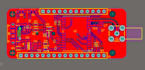
You will receive schematic files, PCB layout, Gerber files, BOM, Pick and Place (CPL), 3D STEP model, and complete manufacturing-ready documentation.
Can you design antenna-based RF systems?
Yes, I can design PCB layouts with antenna integration and RF routing optimized for WiFi, GSM, GPS, and other wireless communication standards.
Which software do you use for RF PCB design?
I use industry-standard tools including Altium Designer, KiCad, EasyEDA, Eagle CAD, CST Studio Suite, and LTspice for design and analysis.
Can you work on high-frequency and multi-layer PCB designs?
Yes, I can design high-frequency and multi-layer RF PCBs with proper stack-up planning, impedance control, and signal routing optimization.
What information do you need before starting?
I need your system requirements such as frequency, wireless protocol, module type, antenna constraints, power requirements, and any reference design if available.
Do you provide manufacturing support?
Yes, all designs are production-ready and optimized for fabrication, including DFM considerations to ensure smooth manufacturing.


