Browse categories
Explore
Fiverr Pro
English
$
USD
PCB Design Embedded Systems IoT Altium Expert Hardware Engineer
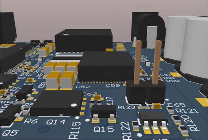
I will design wearable hardware and high density multilayer PCB in Altium Designer
Need a compact, reliable, and production-ready PCB for your wearable device, medical electronics, or embedded product?
I specialize in designing wearable hardware and high-density multilayer PCBs using Altium Designer for healthcare, fitness, IoT, industrial, and consumer electronics applications.
My Services Include:
I focus on compact layouts, battery-powered devices, miniaturized electronics, and high-reliability medical hardware.
Why Choose Me:
What information do you need to start?
Please provide your project requirements, dimensions, block diagram, preferred components, interfaces, and any reference designs.
Can you design PCBs for wearable devices?
Yes. I design compact and low-power PCBs for smart wearables, fitness trackers, health monitors, and portable electronics.
Do you design medical electronics PCBs?
Yes. I develop PCB layouts for diagnostic systems, monitoring devices, healthcare products, and embedded medical electronics.
Can you create HDI and high-density PCB layouts?
Absolutely. I specialize in HDI PCB design, fine-pitch routing, BGA fanout, impedance control, and multilayer stackups.
Which PCB software do you use?
I primarily use Altium Designer and can also work with KiCad when required.
Will I receive editable source files?
Yes. You'll receive Altium source files, schematics, Gerbers, BOM, Pick-and-Place files, and fabrication documentation.
Can you review or redesign an existing PCB?
Yes. I provide PCB review, optimization, redesign, troubleshooting, and manufacturing analysis services.
Are the files ready for PCB manufacturing?
Yes. Deliverables are fully compatible with PCBWay, JLCPCB, Seeed Studio, and other PCB manufacturers.
Can you sign an NDA?
Yes. Confidentiality is guaranteed, and I am happy to sign an NDA before starting your project.