Browse categories
English
$
USD
Connect to your AI
HELLO AND WELCOME!
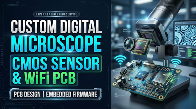
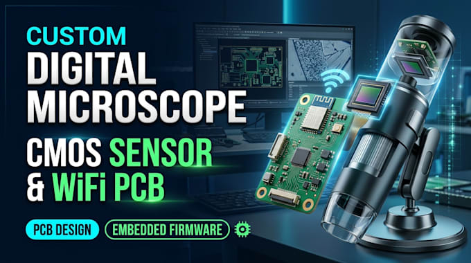
Developing a high-performance digital microscope requires more than connecting a camera sensor to a microcontroller. It involves precise CMOS image acquisition, high-speed data transmission, power integrity, signal conditioning, and reliable wireless communication to deliver clear microscopic images with minimal latency.
What I Will Provide;
Why Choose Me?
Ready to turn your digital microscope concept into a powerful wireless imaging system? message me now and Let's engineer a custom solution with precision CMOS sensor integration, optimized PCB architecture, and reliable WiFi image transmission.!!

Can you design a complete digital microscope PCB?
Yes. I can design the complete electronics, including CMOS sensor integration, WiFi connectivity, power management, and supporting interfaces.
Can you integrate a specific CMOS image sensor?
Yes. I can work with your preferred CMOS sensor, subject to interface compatibility and component documentation.
Can the microscope transmit images over WiFi?
Yes. I can develop a suitable wireless architecture for image streaming and transfer to compatible devices.
Can you develop the embedded firmware?
Yes. I can develop firmware for sensor initialization, image acquisition, communication, and system control.
Will I receive manufacturing files?
Yes. Depending on your package, deliverables can include Gerber files, BOM, schematics, PCB layouts, and design source files.
Can you work on an existing microscope project?
Yes. I can improve, modify, troubleshoot, or redesign an existing digital microscope PCB.
Can you design a compact and portable microscope?
Yes. I can optimize the PCB dimensions, component placement, power architecture, and connectivity for portable applications.