Browse categories
Explore
Fiverr Pro
English
$
USD
PCB Design Engineer, PCB Layout and Electronics Design
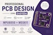
I will design a custom PCB schematic and PCB layout in EasyEDA for your electronic project.
I can help you turn your circuit idea or schematic into a clean, organized and manufacturing-ready PCB design with proper component placement and routing.
What I offer:
Custom PCB schematic design
2-layer PCB layout
Component placement and routing
Power and ground routing
Design Rule Check (DRC)
Gerber files for PCB manufacturing
Bill of Materials (BOM)
EasyEDA source/project files
PDF schematic
3D PCB visualization
PCB projects I can work on:
Power supply and DC-DC converter boards
Sensor and breakout boards
Arduino and ESP-based boards
USB and interface boards
Control and small electronic circuit boards
Software:
EasyEDA
I focus on clean PCB layouts, proper component placement, reliable routing and organized manufacturing files.
Please contact me before ordering and share your schematic, circuit diagram, component list or project requirements so I can understand your project and confirm the scope.
Let's build a clean and professional PCB design for your project!


Specialization:
Circuit design
•
Schematics
•
Layout
•
Gerber
File format:
Gerber
•
STEP
•
SCH
•
Software:
EasyEDA
Interface:
UART
•
USB
•
SPI
•
I2C
What do you need from me to start the PCB design?
Please provide your schematic, circuit diagram, component list, datasheets, board dimensions, and any specific requirements such as connectors, mounting holes, or layer requirements. If you don't have a schematic, contact me first so we can discuss your requirements.
Which PCB design software do you use?
I use EasyEDA for schematic design, PCB layout, routing, DRC checking, and Gerber generation.
What files will I receive?
Depending on the selected package, you can receive PCB layout files, schematic files, EasyEDA source files, Gerber files, BOM, PDF schematic, and 3D PCB visualization.
Do you provide Gerber files for manufacturing?
Yes. Gerber files can be provided with the appropriate package. I also perform DRC checks before preparing the manufacturing files.
Can you design a PCB from my existing schematic?
Yes. I can convert your existing schematic or circuit diagram into a properly organized 2-layer PCB layout with component placement and routing.
Can you design any type of PCB?
I mainly work with small to medium-complexity 2-layer PCB designs such as power boards, DC-DC converters, sensor boards, breakout boards, Arduino/ESP-based boards, and control/interface boards. Please contact me before ordering for complex, multilayer, RF, or high-speed designs.


