Browse categories
English
$
USD
Connect to your AI
PCB Designer Altium Designer Gerber PCB schematic PCB layout
Do you have an existing PCB that needs to be reverse engineered, recreated, or redesigned?
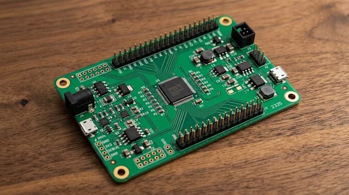
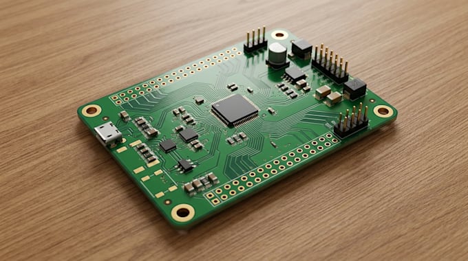
I will help you recover and recreate existing printed circuit board designs using KiCad. Whether you have a physical PCB, clear board images, available Gerber files, or incomplete design documents, I can assess your materials and help turn them into an organized, editable design.
MY PCB REVERSE ENGINEERING SERVICES INCLUDE:
WHAT YOU WILL RECEIVE:
Your deliverables will depend on the package you select and may include an editable KiCad schematic, PCB layout, project files, and BOM. Additional outputs can be agreed upon before ordering.
WHY CHOOSE THIS SERVICE?
I focus on clear communication, organized project files, realistic delivery times, and deliverables matched to your requirements.
Please contact me before ordering complex projects so I can review your requirements and recommend the appropr
What do you need to reverse engineer my PCB?
I need clear photos of the front and back of the board, its dimensions, readable component markings, and any available schematics, Gerber files, or other design documents. Additional information may be needed for complex boards.
Can you recreate a PCB without the original schematic?
Yes, in some cases. I can assess whether the schematic can be reconstructed from the physical board, available images, and trace information. Complete reconstruction cannot be guaranteed if connections are hidden or critical information is missing.
Will I receive editable KiCad files?
Yes. Editable KiCad project files are included in the packages that specify them. The exact files depend on the selected package and agreed scope.
Can you modify or improve my existing PCB?
Yes. I can make agreed changes to an existing design, such as connector placement, component footprints, board dimensions, or layout organization, subject to the available files and package scope.
Can you reverse engineer multilayer PCBs?
Multilayer boards require additional assessment because internal copper layers may not be visible. Please contact me with board details and available files before placing an order.