Browse categories
Explore
Fiverr Pro
English
$
USD
Turn your messy prototype into a Professional & Compact PCB!
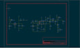
I am an Electronics Engineering student specialized in KiCad. I focus on miniaturizing designs without sacrificing performanceperfect for drones, robotics, or wearables where size matters.
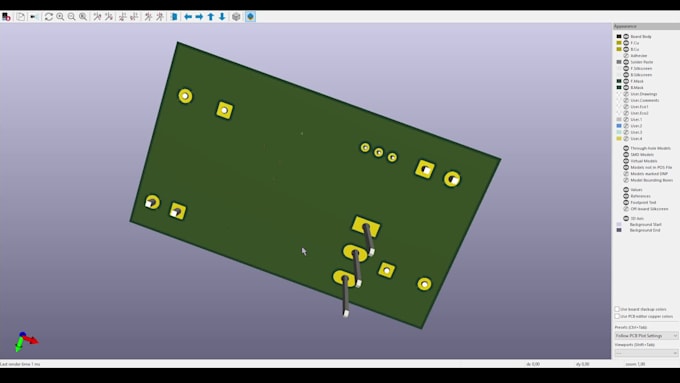
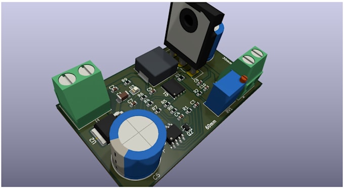
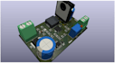
Recent Project: Designed a High-Current Buck Converter compacted into just 60x35mm with optimal thermal management.
My Services: Schematic Capture: From hand-drawn sketches to professional schematics.
PCB Layout: Compact 2-Layer routing (Low Noise & High Efficiency).
Manufacturing Files: Gerber, Drill, & Pick-and-Place (Ready for JLCPCB/PCBWay).
3D Modeling: STEP files for your enclosure design. BOM: Organized Bill of Materials for easy sourcing.
Tools: KiCad, Arduino, ESP32.
️
PLEASE NOTE: Every project is unique. Please CONTACT ME before placing an order to discuss your requirements and get the best price. Let's make your project a reality!

Specialization:
Circuit design
•
Schematics
•
Layout
•
Footprint
•
Gerber
File format:
Gerber
•
STEP
•
VRML
•
SCH
•
Software:
EasyEDA
•
KiCad
•
Arduino
Interface:
I2S
•
UART
•
USB
•
SPI
•
I2C
•
Wi-Fi
Do you ship the physical PCB boards to my address?
No. I provide Digital Design Files (Gerber, BOM, Pick & Place, etc.) only. You can send these files to manufacturers like JLCPCB or PCBWay to get them manufactured.
What files do I need to provide to start the order?
Ideally, a Schematic diagram (PDF or Hand-drawn image). If you only have an idea, please contact me first so we can discuss the circuit design requirements.
Will you keep my project confidential?
Absolutely. I respect your Intellectual Property (IP). I will not share your files with third parties. I am open to signing an NDA (Non-Disclosure Agreement) if needed.