Browse categories
English
$
USD
Connect to your AI
pcb routing, multilayer pcb, gerber files Embedded PCB designs bom Engineer
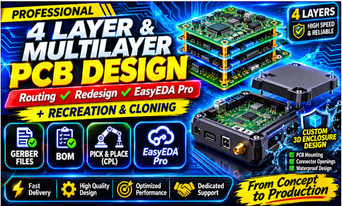
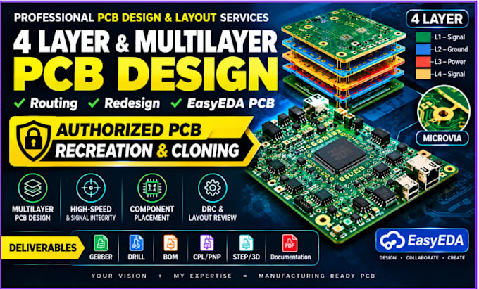
Need a professional 4 layer PCB, multilayer PCB layout or custom PCB redesign with complete manufacturing files and a matching 3D enclosure?
I will design, route and optimize your PCB using EasyEDA Pro with careful attention to component placement, signal routing, power ground planes, rules and manufacturing requirements.
Beyond PCB design, I can also create a custom 3D mechanical enclosure designed to accommodate your PCB, connectors, mounting points and electronic components.
PCB D3SIGN:
PCB MANUFACTURING FILES:
CUSTOM 3D ENCLOSURE & MECHANICAL DESIGN:
Can you design 4-layer and multilayer PCBs?
Yes. I design 4-layer, 6-layer, 8-layer and other multilayer PCBs, depending on project requirements, including component placement, routing, power and ground planes, and DRC checks.
Do you provide Gerber files and BOM?
Yes. I can provide Gerber files, NC drill files, Bill of Materials (BOM), and other required PCB manufacturing documentation.
Can you provide Pick & Place (CPL) files for PCB assembly?
Yes. I can prepare Pick & Place / CPL files alongside the BOM and Gerber files for supported PCB assembly manufacturers.
Do you work with EasyEDA Pro?
Yes. I use EasyEDA Pro for PCB design and can provide the editable project/source files with the manufacturing outputs
Can you design a custom 3D enclosure for my PCB?
Yes. I can design a custom enclosure that fits your PCB and electronic components, including PCB mounting holes, standoffs, internal supports, connector openings, and fastening features.
Can you design waterproof electronic enclosures?
Yes. I can incorporate waterproofing-oriented features such as gasket grooves, O-ring interfaces, sealed connector openings, and cable-entry provisions. Actual waterproof performance depends on materials, manufacturing, assembly, and physical testing
What 3D manufacturing files will I receive?
Depending on your package, I can provide STEP/STP, STL, DXF, 3D enclosure models, and mechanical drawings where required.
Can you redesign or recreate an existing PCB?
Yes. I can redesign, optimize, or recreate an existing PCB using customer-provided files or references, provided you own the design or have authorization to reproduce it.
Can you work from an existing schematic or PCB design?
Yes. I can work from schematics, existing PCB source files, Gerber files, component lists, reference images, and suitable project documentation.
What information do you need before starting?
Please provide your schematic or PCB files, board dimensions, required layer count, component list, connector locations, enclosure requirements, and manufacturing specifications. For complex projects, please contact me before placing an order.