Browse categories
English
$
USD
Connect to your AI
pcb routing, multilayer pcb, gerber files Embedded PCB designs bom Engineer
Hello Valued buyer,
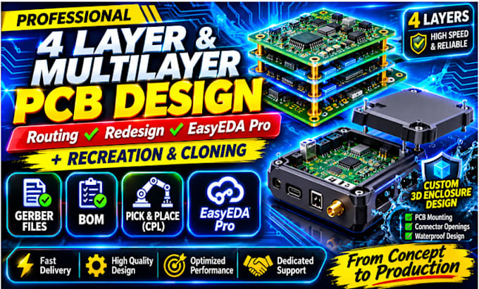
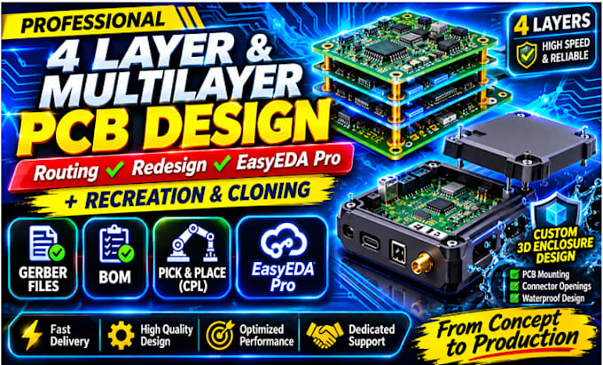
Need a professional 4 layer or multilayer PCB layout, PCB routing, reDesign, or manufacturing-ready Gerber files?
I will design, route, redesign, and optimize your PCB using EasyEDA or other supported PCB design tools, based on your project requirements.
Services includes:
I can work from schematics, existing PCB source files, Gerbers or other suitable project.
For PCB redesign, reverse engineering, or cloning, please confirm that you own the board/design or have authorization to reproduce it.
Please contact me before ordering complex projects and send your schematic or PCB files, board dimensions, layer count, component information, Thanks
Can you design a 4-layer PCB?
Yes. I can design and route 4-layer PCBs based on your schematic, component information, board dimensions, and manufacturing requirements.
Can you design multilayer PCBs?
Yes. I can work on 4 layer and other multilayer PCB projects depending on complexity and requirements.
Can you design PCB in EasyEDA?
Yes. I can create or modify PCB layouts in EasyEDA when the project requirements and source files are suitable.
Can you redesign my existing PCB?
Yes. I can review, modify, optimize, and reroute an existing PCB design for improved layout or manufacturing requirements.
Can you provide Gerber files?
Yes. Gerber and drill files can be included according to the selected package and manufacturer requirements.
Can you recreate or clone an existing PCB?
Yes, for boards and designs that you own or are authorized to reproduce. I can recreate suitable PCB information into a usable schematic/layout and manufacturing package.
Can you work from Gerber files?
Yes. Depending on the files provided, I can review them and determine what can be recreated, modified, or prepared for manufacturing.
Can you provide BOM and Pick and Place files?
Yes, when the required component information is available and the selected package includes these deliverables.
What do you need before starting?
Please provide the schematic or existing PCB files, board dimensions, layer count, component/BOM information, manufacturer requirements, and any mechanical or electrical constraints.
Should I contact you before ordering?
For complex 4-layer, multilayer, redesign, reverse-engineering, or PCB recreation projects, yes. Please contact me first so I can review the scope and provide the appropriate offer.