Browse categories
Explore
Fiverr Pro
English
$
USD
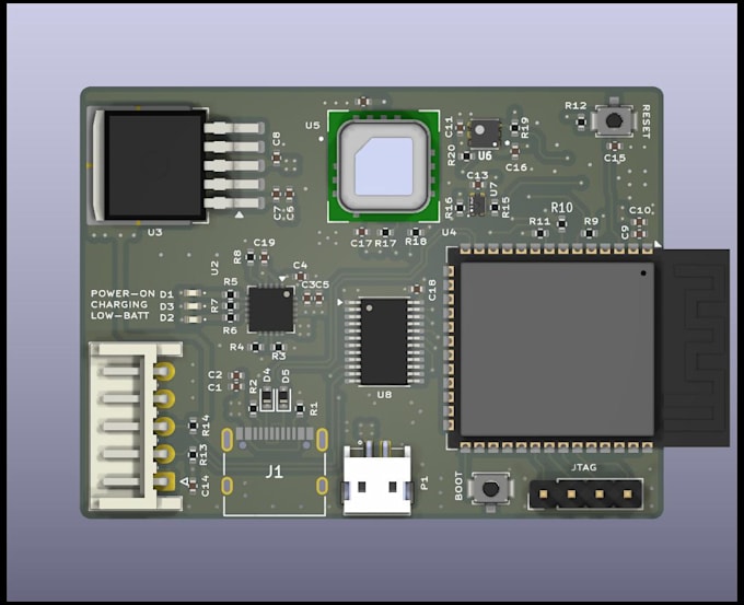
I turn complex circuit concepts into high-performance, production-ready hardware. Are you looking for a PCB designer who does more than just "connect the dots"? A great design is about signal integrity, thermal management, and minimizing costs.
I specialize in taking products from napkin sketches to final Gerber files, ensuring every board is optimized for mass production. Whether youre building a compact IoT wearable, an RF synthesizer, or a high-power controller, I focus on "First-Time-Right" engineering to save you time and expensive revision costs.
Technical Toolkit:
Why Work With Me?
Lets bring your vision to life!

What do I need to start a PCB project?
You just need to share your idea or any particular specification you have or want.
Do you do revisions?
Unlimited revisions included with every package
What will I receive?
Complete Gerber with KiCad files, BOM, CPL file, PDF documentation and 3D renders.
| (2) | ||
| (0) | ||
| (0) | ||
| (0) | ||
| (0) |
brianbigdelle

United States
great turn around time, perfect results.
Up to $50
Price
3 days
Duration
cubanme
United States
This was my first time using Fiverr, and it was a great experience working with this freelancer. I think I will try to find more of these types of projects to do in the future, and I will definitely try working with this freelancer again
Up to $50
Price
4 days
Duration
| (2) | ||
| (0) | ||
| (0) | ||
| (0) | ||
| (0) |
brianbigdelle
United States
great turn around time, perfect results.
Up to $50
Price
3 days
Duration
cubanme
United States
This was my first time using Fiverr, and it was a great experience working with this freelancer. I think I will try to find more of these types of projects to do in the future, and I will definitely try working with this freelancer again
Up to $50
Price
4 days
Duration
