Browse categories
Explore
Fiverr Pro
English
$
USD
Smart Designs, for Real World Solutions
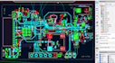
I will professionally review your PCB schematic and layout to catch critical design issues before they become costly mistakes. I focus on manufacturability, reliability, and signal/power integrity so your board assembles right the first time.
What I check:
Deliverables
Why choose me?
Order instructions: Choose a package, attach your files and tell me what to focus on. Ill return a clear action list you can hand to your engineer or manufacturer.


What file formats do you accept?
Native files (Altium, KiCad, Eagle, Orcad, Proteus), Gerbers, Bom (CSV), PDFs, and images.
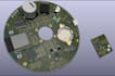
I only have Gerbers. Can you still review?
Yes — I can do a full DFM and layout review from Gerbers.
Will you edit my files directly?
I will supply annotated suggestions and specific change instructions. File edits can be offered as a separate gig or gig extra.


