Browse categories
Explore
Fiverr Pro
English
$
USD
PCB Layout Designer using EasyEDA and KiCad for 1 to 4 layer boards
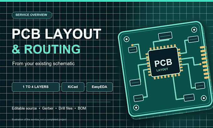
I will create a PCB layout from your existing schematic using EasyEDA or KiCad. I work on 1 to 4 layer boards, including component placement, routing, board outlines and connector positioning.
Basic package ($15): a simple 2-layer PCB with up to 25 components, delivered in 14 days with 3 revisions. You will receive the editable project/source file, Gerber files, drill files and a BOM.
Please send your schematic, component and footprint information, board dimensions, connector and mounting-hole positions, preferred PCB manufacturer, and any electrical or mechanical constraints before ordering. I will confirm the scope first.
High-speed, RF/antenna, SD-card, and complex 3 to 4 layer projects need a custom quote. This Gig starts from a supplied schematic; schematic capture, physical PCB fabrication and assembly are not included.

Specialization:
Layout
•
Gerber
File format:
Gerber
Software:
EasyEDA
•
KiCad
