Browse categories
Explore
Fiverr Pro
English
$
USD
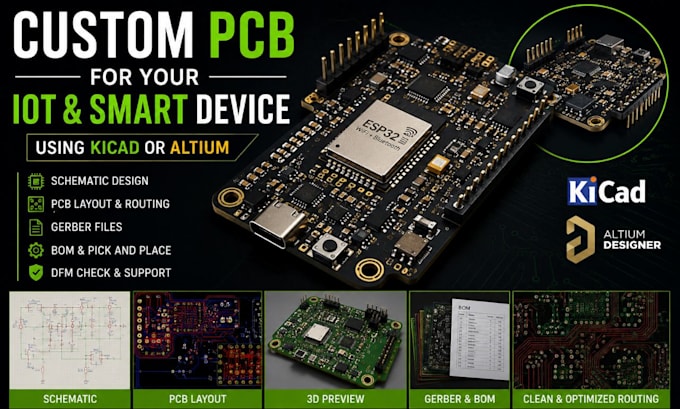
From schematic to board, I make your hardware work
Building an IoT device but stuck on the PCB? I design it for you.
I'm a PCB design engineer with 7+ years delivering production-ready boards for USA hardware startups, IoT product teams, and embedded systems developers. I specialize in IoT and smart device PCBs, the kind that need to be compact, power-efficient, FCC-aware, and ready for mass production.
Tools I use: KiCad, Altium Designer, EasyEDA, your choice. Simulation via LTspice. Gerber files formatted for JLCPCB, PCBWay, OSH Park, and MacroFab.
Every design includes:
I serve IoT startups building connected products, smart home hardware developers, wearable teams, and engineers prototyping Arduino or ESP32-based devices. Premium adds 4-layer design, EMI mitigation, and full DFM optimization for first-pass manufacturing success. Share your project brief, I'll confirm feasibility and timeline before you order.