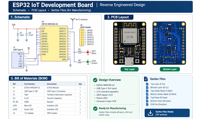
I reverse engineer existing PCB boards into editable circuit schematics, PCB layouts and Gerber files for repair, redesign, component replacement or manufacturing. I can work from physical boards, high-resolution photos, scans, component markings or existing documentation to reconstruct connections & recreate the board where technically feasible.
WHAT I REVERSE ENGINEER
- Single, double & multilayer PCB designs
- Circuit tracing & schematic reconstruction
- Component identification, values & footprints
- PCB layout recreation from physical references
- Power, signal, connector & interface circuits
- Legacy, obsolete & discontinued electronics
PCB RECONSTRUCTION
- Trace, via & net connectivity mapping
- Board dimensions, mounting holes & placement
- Footprint correction & component alternatives
- Schematic ERC & PCB DRC verification
- DFM/DFA checks for modern fabrication
- JLCPCB/PCBWay manufacturing preparation
DELIVERABLES
- Editable schematic & PCB source files
- Gerber + NC Drill package
- BOM with identified component references
- Pick-and-Place/CPL files
- PDF schematic + optional STEP/3D model
- Reconstruction notes & unresolved findings
Contact me with clear board photos, dimensions & available document.