Browse categories
Explore
Fiverr Pro
English
$
USD
PCB Design Expert
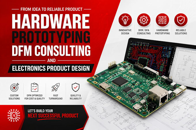
Most PCB designs fail at manufacturing not because the schematic is wrong, but because nobody thought about how the board would actually be built. Wrong footprints, untestable layouts, components that are out of stock or impossible to hand-solder, trace widths that fail production tolerances. I fix all of that before it costs you money.
I provide hardware prototyping and DFM (Design for Manufacturing) consulting for engineers, startups, and product companies who want to get from idea or prototype to a manufacturable product without expensive spins.
Here's where I add value:
DFM audits that flag real manufacturing risks before you send Gerbers, Component selection and BOM optimization for cost, availability, and replaceability, Footprint verification against manufacturer datasheets, Panelization guidance for production runs, Test point placement for in-circuit testing, Stackup recommendations for your layer count and impedance needs, Communication with JLCPCB, PCBWay, or your chosen fab during production..

What do I need to send for a DFM review?
Your Gerber files, schematic, and BOM. Additional files like the native PCB project (KiCad, Altium, EasyEDA) are helpful but not required.
Can you help with component shortages and finding replacements?
Yes. I check availability on Mouser, DigiKey, and LCSC and suggest drop-in or near-drop-in replacements when needed.
Do you work with JLCPCB's parts library for SMT assembly?
Yes. I can align your BOM and footprints specifically with JLCPCB's in-stock SMT library to minimize extra costs.
