Browse categories
Explore
Fiverr Pro
English
$
USD
PCB Design Expert, EasyEDA, IoT, Arduino And Power Electronics
Looking for a reliable PCB designer in EasyEDA who can take your idea all the way to manufacturing-ready files? I provide professional PCB design services focused on accuracy, clarity, and real-world production.
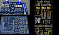
I design clean schematics and well-routed PCBs that follow proper design rules and fabrication standards. Whether you need a simple prototype or a complex multilayer board, I ensure your design is optimized for performance, cost, and manufacturability.
What I can do for you:
My designs are suitable for JLCPCB and other manufacturers, helping you move smoothly from concept to production without delays or errors.
I work with hobbyists, startups, and businesses on IoT boards, power supplies, control circuits, and embedded systems.
Please message me before ordering to confirm board size, layers, and component count so I can deliver exactly what you need.

File format:
Gerber
•
SCH
Software:
EasyEDA
•
KiCad
Interface:
HDMI
•
MIPI DSI/CSI
•
I2S
•
SPI
•
I2C
•
BLE
•
GSM/GPRS
Do you provide manufacturing-ready files?
Yes, I deliver production-ready Gerber files, BOM, and Pick & Place files compatible with PCB manufacturers.
Can you design multilayer PCBs?
Yes, I design 2-layer, 4-layer, and multilayer PCBs in EasyEDA.
Can you modify or fix an existing PCB?
Absolutely! I can edit, optimize, or fix existing EasyEDA PCB designs.
