Browse categories
Explore
Fiverr Pro
English
$
USD
pcb design, embedded system and firmware development
Hello there!
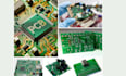
I Designed advanced PCB layouts involves more than just placing components it requires precision, optimization, and a deep understanding of circuit behavior to ensure performance, reliability, and manufacturability.
From schematic interpretation to compact routing and production ready files, I deliver high quality PCB layout tailored for real world applications.
Are you're building a prototype or preparing for mass production, I will help turn your circuit into a clean, efficient, and fabrication ready PCB layout.
What I Will Provide:
Why Choose Me?
NOTE: MESSAGE ME BEFORE PLACING ORDER

What do you need to start my PCB design?
I need your schematic, project requirements, board size constraints, and any specific components or preferences.
Can you design PCB from my idea only?
Yes. I can convert your idea into a schematic and then design a complete PCB layout.
Which PCB design software do you use?
I use tools like Altium Designer, KiCad, and Eagle depending on your project requirements.
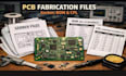
Will I get fabrication files for manufacturing?
Yes. You will receive complete Gerber files, drill files, and other files required for PCB fabrication.
Do you provide BOM (Bill of Materials)?
Yes. I provide a detailed BOM with component specifications and sourcing information.


