Browse categories
Explore
Fiverr Pro
English
$
USD
HELLO WELCOME TO MY GIG
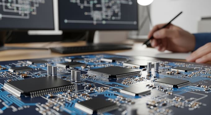
I will design EMI/EMC optimized PCB layouts to reduce noise, improve performance, and help your product pass certification standards. Poor PCB design is one of the main reasons devices fail EMI/EMC testing and this is where I come in.
I apply industry-proven techniques like proper grounding, shielding, filtering, and stack up planning to minimize interference and ensure stable operation.
SERVICES INCLUDE:
- Multi-layer stack up planning for signal integrity
- Precise return path and ground plane optimization
- Differential pair routing and impedance matching
- Strategic decoupling and filtering placement
- Cross-talk and EMI radiation mitigation
- Full manufacturing files and BOM generation
HOW IT WORKS
1. You send the schematic and board constraints
2. I design the layout with EMC-first principles
3. Final delivery with all production files
Message me before ordering to discuss your project!


Do you handle the schematic design as well?
This gig is specifically for PCB layout based on an existing schematic. If you need schematic creation or circuit simulation, please message me for a custom quote.