Browse categories
Explore
Fiverr Pro
English
$
USD
Hello and welcome to my gig
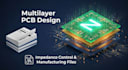
Getting a high speed PCB right is about more than just connecting dots. If your signals aren't clean or your stack up is off, the board won't work as expected. I focus on making sure your multilayer layout is stable, manufacturable, and electrically sound from the start.
I treat every project like my own hardware. Whether it is a dense 4-layer IoT device or a complex 8-layer board with high-speed differential pairs, I handle the routing grit so you do font have to. I do not just auto-route; I manually place every critical trace to maintain signal integrity.
Services Include:
How it works:
Message me with your project details and let's get it !!!
Can you help me choose the right components?
Yes, I select parts based on availability at major distributors like Mouser or Digi key to ensure you can actually get the board built.
Which software do you use for the design?
I primarily use Altium Designer and KiCad. If you have a specific preference for your project, just let me know.


