Browse categories
Explore
Fiverr Pro
English
$
USD
Embedded Hardware And PCB Development
Need a reliable engineer to build a USB-C board, USB hub PCB, or custom development board without signal or power delivery issues?
I create custom USB-C boards, USB hub PCBs, USB interface boards, and computer development/carrier boards for hardware startups, embedded systems projects, and product prototypes. Every layout is built with controlled-impedance differential pair routing, proper power delivery negotiation, ESD protection, and a layer stackup suited to your board's complexity.
With experience across multilayer PCB layout and embedded hardware, I understand how critical grounding, connector shielding, and trace routing are for stable USB performance issues that cause data errors, EMI, or power faults when handled incorrectly.
What You'll Get:
Message me your project details & let's build a reliable, professional board.
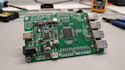
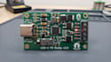
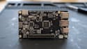
Do I need to provide a schematic, or can you create one from scratch?
Either works send your existing schematic for layout, or share your requirements and I'll design the schematic first before moving to layout.
How many layers will my USB-C or USB hub board need?
It depends on speed and complexity most USB-C and USB hub designs require 4+ layers for proper impedance control and ground planes. I'll recommend the right stackup after reviewing your project.
Can you help with USB Power Delivery (PD) circuit design?
Yes, I handle PD controller integration, voltage negotiation circuitry, and current path design for reliable power delivery.
Will my board be optimized to prevent signal integrity issues?
Yes, controlled-impedance routing, proper grounding, and ESD protection placement are standard parts of my design process.
Can you design a carrier board for a specific SoC or Compute Module?
Yes, send me the module's datasheet or reference design and I'll build a custom carrier board around it.
What software do you use, and can I request a specific one?
I work across Altium Designer, KiCad, Eagle, EasyEDA, and more — let me know your preference and I'll accommodate it.
Do you test or simulate the design before finalizing it?
Yes, simulation and design rule checks (DRC) are performed to catch issues before Gerber files are generated.
Can you work with my existing PCB and just make revisions or fixes?
Yes, share your current design files and I'll review and revise as needed.


