Browse categories
Explore
Fiverr Pro
English
$
USD
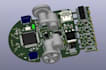
Your Idea! My Circuits!! One Perfect Product!!!
I'm Owen Flisnik, a Mechatronics and Electrical Engineer with 5 years of experience delivering clean, precise, and production-ready PCB designs across IoT, industrial, EV, and consumer electronics. If your project has been delayed by poor layouts, fabrication errors, or unreliable designers, that stops here.
Problems I solve:
What you receive:
Every file I deliver is fabrication ready, thoroughly checked, and built to perform exactly as intended.
Message me before placing your order, let's discuss your project and make sure we deliver exactly what your product needs.


What makes your PCB design service different from others on Fiverr?
Beyond just designing boards, I bring full engineering insight to every project. Every design is DRC, ERC, and DFM verified before delivery, meaning your board is not just designed, it is engineered to be manufactured, assembled, and perform reliably in the real world.
Do you design both simple and complex PCBs?
Yes. I handle everything from basic single layer boards for simple circuits to complex multi-layer designs involving high speed signals, power management, RF components, and dense component placement. No project is too simple or too advanced.
Will my design be ready to send directly to a PCB manufacturer?
Every deliverable includes fully verified Gerber files, drill files, and fabrication notes that meet standard manufacturer requirements. You can send the files directly to any PCB fab house JLCPCB, PCBWay, or your preferred manufacturer.
Can you optimize an existing PCB layout that is not performing well?
Yes. If your current board has signal integrity issues, poor routing, EMI problems, thermal concerns, or simply needs a cleaner layout, I can audit, diagnose, and redesign it to perform at its best.
What if my project requires components that are hard to source?
Component availability is always considered during the design process. I select components with good market availability and suggest alternatives where needed, ensuring your BOM is practical and ready for procurement without supply chain headaches.
Can you work under NDA to protect my project?
Yes, Client confidentiality is something I take seriously. I am happy to sign an NDA before any project discussion begins. Your designs, ideas, and intellectual property remain completely yours.
What happens if the PCB manufacturer raises a technical query about my files?
I've got you covered. If your manufacturer raises any technical questions or flags issues with the delivered files, reach out to me directly and I will resolve it promptly. Your project doesn't end at delivery.
Do you design PCBs for regulatory compliance such as FCC or CE?
Yes. For products targeting regulated markets, I design with compliance in mind, considering EMI shielding, trace spacing, grounding strategy, and component placement that align with FCC, CE, and other standard requirements, giving your product a smoother path through certification.


