Browse categories
Explore
Fiverr Pro
English
$
USD
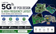
Embedded firmware and PCB design built for performance and reliability
Struggling to get your 5G or high-frequency wireless device working flawlessly?
I provide 5G RF PCB design and high-frequency layout that ensures optimal signal integrity, minimal EMI, and precise impedance control. I solve the headaches of prototype failures and layout issues so your device performs exactly as intended.
This gig is ideal for:
What you will get:
Software and Tools used:
Deliverables:
Ready to make your wireless project a success? Message me now, send your requirements and get expert RF PCB design today!
Thank you!

Can you design a 5G RF PCB for my specific device specifications?
Yes! I customize every RF PCB design to your exact device requirements, including frequency, impedance, stack-up, and signal integrity. Just provide your schematic or specifications, and I’ll ensure optimal performance.
What deliverables will I receive after the order?
You’ll get complete Gerber files, PCB schematics, 3D PCB models, and a signal integrity/layout report—everything needed for prototyping or manufacturing.
Which software/tools do you use for RF PCB design?
I use Altium Designer, KiCad, HFSS, and CST Studio Suite to ensure professional, accurate, and simulation-tested high-frequency PCB layouts.
