Browse categories
English
$
USD
Connect to your AI
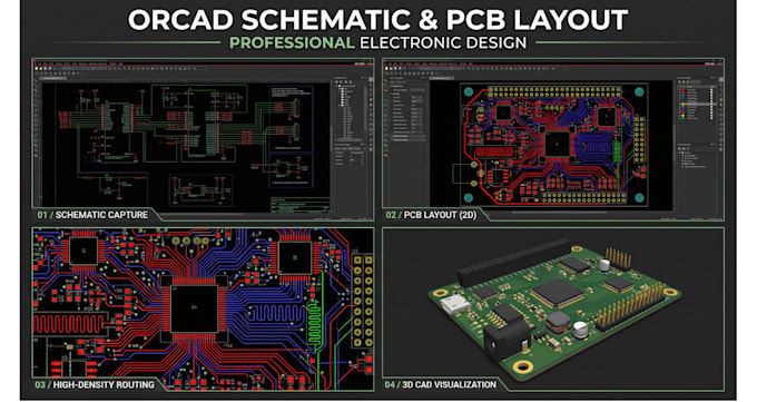
Need reliable OrCAD PCB design that is clear, electrically consistent, and ready for fabrication? I can turn your circuit concept or schematic into a professional PCB design with organized manufacturing outputs
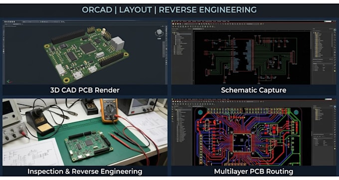
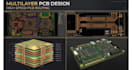
I provide Cadence OrCAD schematic capture, PCB layout, multilayer PCB design, component placement, routing, Gerber generation, BOM preparation, and design rule checks. I can also assist with high-speed PCB layout, rigid-flex deslgn, PCB debugging, DFM analysis, and reverse engineering. Each project is reviewed against your requirements, board constraints, and manufacturing needs
I can help you optimize your PCB design service with OrCAD board routing, OrCAD DRC fixing, OrCAD PCB repair, PCB schematic recreation, PCB deslgn rule correction, PCB layout optimization, PCB footprint correction, legacy PCB redesign, PCB netlist correction, PCB manufacturing review, high-density PCB routing, rigid-flex circuit layout, and PCB component replacement to ensure accurate, reliable, and manufacturing-ready electronic deslgns
Please share your schematic or circuit details, layer count, board dimensions, and target manufacturer
Message me before ordering.
Specialization:
Circuit design
•
Schematics
•
Layout
•
Gerber
File format:
Gerber
•
SCH
•
Circ
•
Pcbdoc
Software:
Cadence OrCAD
What information do you need to start my OrCAD PCB design?
I need your circuit schematic, project requirements, component list, board dimensions, desired layer count, and any reference files available.
Can you provide manufacturing-ready Gerber files?
Yes. I can provide Gerber, NC drill, BOM, and editable OrCAD project files according to the agreed package and project requirements.
Can you work on existing PCB designs or fix PCB errors?
Yes. I can help with PCB debugging, DRC error correction, existing board modifications, reverse engineering, and PCB layout optimization, depending on the available source files.