Browse categories
Explore
Fiverr Pro
English
$
USD
Professional PCB Design Engineer Altium, KiCad, Eagle, OrCAD EasyEDA
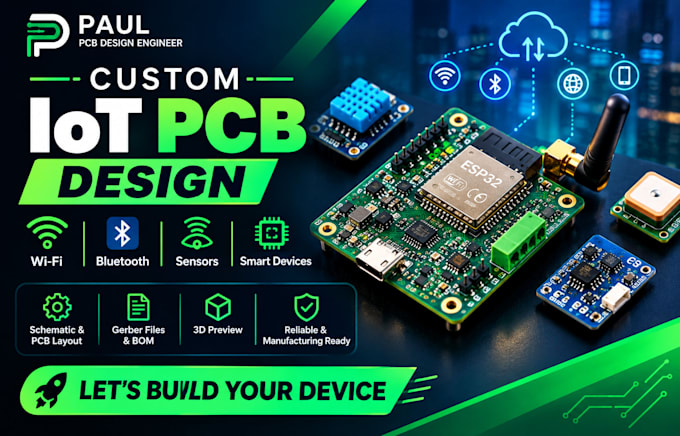
Looking for a professional IoT PCB designer for your smart device or wireless electronics project?
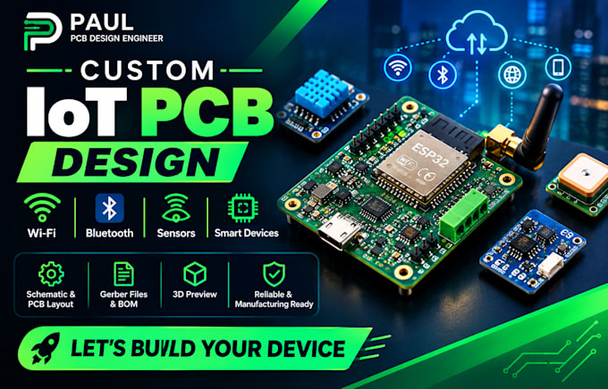
I will design custom IoT PCBs for sensors, smart devices, wireless monitoring systems, and connected electronics using Altium Designer, KiCad, Eagle, OrCAD, or EasyEDA.
My services include:
I focus on clean layouts, reliable design practices, and manufacturing-ready deliverables tailored to your requirements.
Ready to build your smart device? Contact me today to discuss your project and let's turn your idea into a professional IoT PCB!
What IoT devices can you design?
I can design sensor boards, smart controllers, monitoring systems, and custom connected electronics.
Can you design Wi-Fi and Bluetooth hardware?
Yes, depending on the module and project requirements.
Can you work with an existing schematic?
Yes, I can use your existing schematic or project files as a starting point.
Do you provide manufacturing files?
Yes, Gerber, drill, BOM, and other files are available according to your package.
Can you work from an idea?
Yes. Share your concept and requirements so I can assess the project before you order.