Browse categories
Explore
Fiverr Pro
English
$
USD
ELECTRONIC ENGINEERING AND EMBEDDED SYSTEM
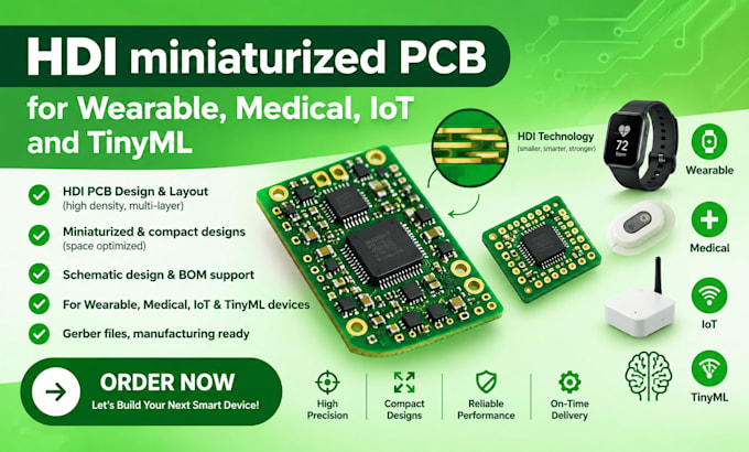
Build compact, high-performance electronics with an HDI PCB engineered for space constrained wearable, medical, IoT and TinyML applications. I handle complex layouts where size, signal integrity, component density and reliable manufacturing matter.
Services I offer:
Why choose me:
Deliverables:
Send your schematic, board requirements, dimensions or reference design to discuss the project scope and move toward a compact, production ready PCB.
What type of PCB projects do you handle?
I work on HDI, compact, wearable, medical, IoT, BLE, MEMS and TinyML PCB projects.
Can you reduce the size of an existing PCB?
yes. I can optimize component placement, routing, layer usage and interconnects to achieve a more compact board.
Do you support HDI technologies?
Yes. Projects can include microvias, via-in-pad, fine-pitch components and high-density routing.
Can you handle BLE and sensitive RF signals?
Yes. I can work with RF-aware layouts, controlled impedance, antenna interfaces and signal-sensitive routing.
What files will I receive?
Depending on the package, deliverables can include source PCB files, Gerbers, drill files, BOM, Pick & Place files and DRC/DFM documentation.