Browse categories
Explore
Fiverr Pro
English
$
USD
PCB Designer , Electrical Engineer
About this Gig
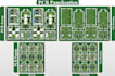
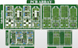
Welcome to your solution for efficient PCB Panelization/Array services. I offer variety of services to optimize your PCB design for manufacturing, saving you time and resources.
Services Offered:
Expertise:
Deliverables:
Why Choose Me:
Optimize your PCB production with confidence. Contact today to discuss your project.

Specialization:
Circuit design
•
Schematics
•
Layout
•
Footprint
•
Gerber
File format:
Gerber
•
STEP
•
BRD
•
3DS
•
Software:
Allegro
•
Altium Designer
•
Eagle CAD
•
EasyEDA
•
KiCad
Interface:
HDMI
•
I2S
•
UART
•
USB
•
I2C
Will you help/guide me in placing an order for PCB Fabrication/Manufacturing or will you place an order for me ?
Yes, I will guide you through placing the order or if you want I can place the order for you and have the PCBs delivered to your address.
Can a buyer negotiate a price lower than the one mentioned in your gig? Will you provide repeat buyers with discounts?
Yes, price negotiation will not be an issue. Repeated costumers will be provided with excellent discounts.
What files do you need to do PCB Penalization & PCB Array?
You have to provide me with PCB Layout for Array Design & for PCB Penalization, you have to provide me with the Layouts of all the PCBs you want on a single panel.
What specifications do I need from you to start the designing process?
Kindly specify the PCB Panel shape, No. of PCBs to be placed on single panel (No. of Columns / Rows), dimensions (Column / Row Spacing), custom features (e.g., cutouts, fiducial marks etc.), and the technique/methodology (V-Score / V-Cut, Tab Routing etc.) to be used for Penalization.
What files you will provide me and what do I do with that?
To manufacture the PCB all you need is the GERBER file, a zip file that you can send to any PCB manufacturer to fabricate the PCB. Additionally, I will provide Step 3D file for mechanical design along with DWG/DXF file. Design documentation including 3D-PDF will also be provided.
Will you add Markers/Fiducials & Tooling Holes to the panel?
Yes, I will add Markers/Fiducials & Tooling Holes to the PCB panel for reference, accuracy & alignment.
Which tool will you use for Designing PCB Panels / Array?
My primary tool for PCB Designing is Altium Designer but if you want I can design your panels in Cadence Allegro, KiCAD, Autodesk Eagle, EasyEDA, Proteus, SolidWorks PCB, or any tool of your choice.


