Browse categories
Explore
Fiverr Pro
English
$
USD
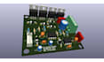
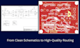
Need a professional, production-ready PCB? I will transform your schematic into a clean, manufacturing-ready KiCad layout.
I am a PCB Design Engineer with 5+ years of experience in microelectronics and EMC-compliant hardware design.
WHAT I OFFER:
Schematic to PCB Layout (up to 4 layers / 100 components)
Component placement, routing & custom footprint creation
Design Rule Checks (DRC) for your manufacturer (JLCPCB, PCBWay, etc.)
EMC-compliant layouts
WHAT YOU GET:
Production-ready Gerber & Drill files
Bill of Materials (BOM)
Pick & Place / Centroid files
KiCad source files & 3D STEP model
PACKAGES:
BASIC ($5): 2 Layers, up to 25 components. Ideal for small DIY/breakout boards.
STANDARD: Up to 4 Layers, up to 50 components. For standard MCUs & IoT.
PREMIUM: Up to 4 Layers, up to 100 components. Includes high-speed/EMC routing.
1 DAY DELIVERY:
You can order the Basic package directly if your schematic is ready! For custom requirements, feel free to message me.
SPECIAL SERVICE
Need a case for your board? I design matching 3D printable enclosures. Avoid alignment issues and save time. Contact me for a custom bundle offer!
Let's bring your project to life! Message me now.


Specialization:
Circuit design
•
Schematics
•
Layout
•
Footprint
•
Gerber
File format:
Gerber
•
SCH
•
Software:
KiCad
Interface:
USB
•
I2C


