Browse categories
Explore
Fiverr Pro
English
$
USD
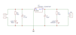
Do you have an electronic schematic but need a professional PCB layout?
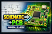
I will convert your schematic diagram into a clean and manufacturable 2 layer PCB layout using EasyEDA.
This service is perfect for hobby projects, Arduino boards, IoT devices, or custom electronics that need a reliable PCB design ready for fabrication.
What I Will Do
What You Will Receive
Your PCB will be ready to manufacture at services like JLCPCB or PCBWay.


Specialization:
Circuit design
•
Schematics
•
Layout
•
Gerber
File format:
Gerber
•
Software:
EasyEDA
Interface:
Wi-Fi
What files do you need to start the PCB design?
Please send your schematic diagram, component list (if available), and any board size requirements.
What files will I receive?
You will receive Gerber files, EasyEDA project files, and optionally a Bill of Materials (BOM).
Is the PCB ready for manufacturing?
Yes, the PCB will be checked with design rules and prepared for manufacturing services like JLCPCB or PCBWay.


