Browse categories
Explore
Fiverr Pro
English
$
USD
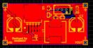
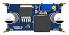
I will design a 2-layer PCB in EasyEDA
Are you looking for a reliable and high-quality 2-layer PCB design for your electronics project? Youre in the right place!
I will design a 2-layer PCB using EasyEDA, optimized for performance, manufacturability, and cost-efficiency.
What I Offer:
Custom 2-layer PCB design in EasyEDA
Schematic design
Clean and optimized component placement
Proper routing with signal integrity in mind
Ground planes and power planes optimization
Design Rule Check (DRC) verification
Gerber files ready for manufacturing
Bill of Materials (BOM)
Pick and Place file (if required)
Whether you need a simple board or a more complex project, Im here to help bring your idea to life.
Contact me before placing an order to discuss your project requirements.
Lets turn your circuit into a professional PCB!


Specialization:
Circuit design
•
Schematics
•
Layout
•
Gerber
File format:
Gerber
•
Software:
EasyEDA
Interface:
Wi-Fi
Will the PCB be ready for manufacturing?
Yes. I provide complete, manufacturing-ready Gerber files compatible with manufacturers like JLCPCB, PCBWay, and others.
Do you provide revisions?
Yes. I offer revisions depending on the package selected. Minor adjustments are always included.
How long does delivery take?
Delivery time depends on the complexity of the project. Simple boards can be completed faster, while more complex designs may require additional time.


