Browse categories
Explore
Fiverr Pro
English
$
USD
Turning Ideas Into Products and Websites
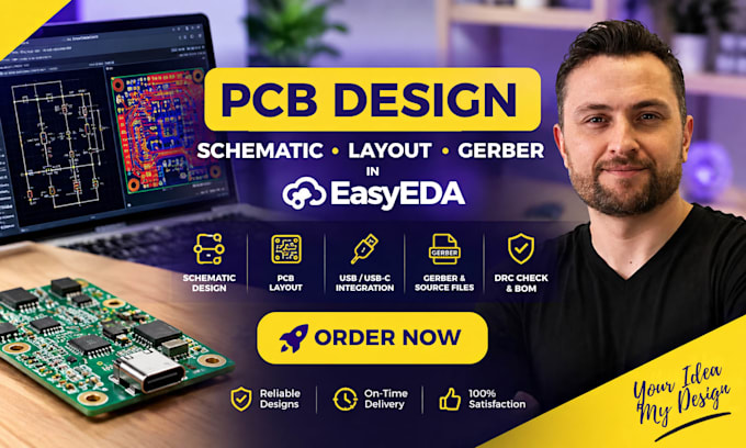
WELCOME TO MY PCB GIG!
Is your PCB schematic incomplete, difficult to route, or not ready for manufacturing? A poorly designed PCB can cause connection errors, signal issues, component fitting problems, and costly prototype revisions.
I can turn your circuit idea or existing schematic into a clean, organized, and production-ready PCB design using EasyEDA.
My PCB design service includes:
Whether you're developing a simple prototype, USB device, IoT project, or custom electronic product, I focus on keeping the design organized, practical, and ready for the next stage.
You'll receive the relevant design files clearly organized so you can review, modify, or send them for fabrication.
Have a PCB project in mind? Send me your schematic, requirements, or even a basic circuit idea, and lets discuss the right design approach before you order.


Can you design a PCB from my circuit schematic?
Yes. I can convert your schematic into a properly organized PCB layout with component placement and routing.
Can you create the schematic from my circuit idea?
Yes. If you provide the circuit requirements, components, or reference diagram, I can create the schematic in EasyEDA.
Can you design a USB PCB?
Yes. I can work on PCB designs involving USB and USB-C connections, depending on your circuit requirements.
Can you design a single layer PCB?
Yes. Simple single layer PCB layouts are suitable for my Basic package.
Can you check my PCB for errors?
Yes. I can perform design checks such as Design Rule Check (DRC) and review common layout issues.
Can you design a compact PCB?
Yes. I can optimize component placement and routing around your available board dimensions and enclosure constraints.
Can you work from a breadboard or hand-drawn circuit?
Yes. You can provide a clear diagram, image, reference design, or component list for me to review.
Can you prepare my PCB for manufacturing?
Yes. I can prepare the necessary design and manufacturing files, including Gerbers, depending on the project scope.