Browse categories
Explore
Fiverr Pro
English
$
USD
pcb design, embedded system and firmware development
Hello there!
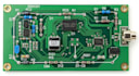
Are you looking for a precise, high performance RF detector circuit PCB design with optimized high frequency layout?
I specialize in designing advanced RF detector circuits and professional grade PCB layouts that ensure signal integrity, minimal noise, and optimal performance for high frequency applications.
What I Will Provide:
Why Choose Me:
NOTE:
Lets bring your RF project to life with a clean, efficient, and high-performance PCB design.
Send me a message now with your requirments, and lets get started on building your rf detector circuit the right way


_compressed (1)_kuiwii.jpg)
Do you provide both schematic and PCB design?
Yes, I provide both schematic design and PCB layout optimized for RF and high frequency performance.
What files will I receive?
You will receive Gerber files, BOM (Bill of Materials), PCB layout files, and assembly files depending on your package.
Can you work with existing circuit designs?
Yes, I can redesign, improve, or optimize your existing RF detector circuit and PCB layout.
Do you ensure high-frequency performance?
Yes, I follow RF design rules like impedance control, grounding, and EMI reduction for stable performance.
What information do you need to start?
I need your project requirements, circuit idea (if available), frequency range, and any reference design or constraints.


