Browse categories
English
$
USD
Connect to your AI
pcb design
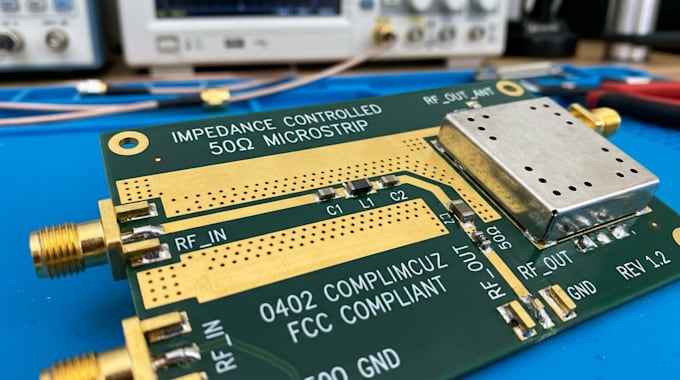
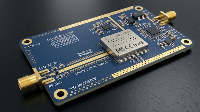
Great RF performance doesn't happen by accident it starts with the right impedance, clean routing, and a PCB layout de.signed with signal integrity in mind.
Are you developing an RF device and need controlled impedance microstrips for reliable high frequency performance? I can help turn your de.sign requirements into a carefully planned PCB layout with signal integrity and manufacturability in focus.
WHAT YOU CAN EXPECT:
WHAT MAKES ME DIFFERENT?
I focus on the engineering details behind the layout, not just how the board looks. I prioritize clear communication, careful de.sign decisions, and practical deliverables tailored to your project.
DELIVERABLES:
LET'S GET STARTED!
Send me your stackup, target impedance, operating frequency, and project requirements. Let's work together to build an RF PCB design ready for the next stage of development!

What information do you need to start my RF PCB design?
Please provide your schematic, PCB requirements, operating frequency, target impedance, layer stackup, and preferred design software, if available.
Can you design controlled impedance RF microstrips?
Yes! I can help design RF microstrip traces using your target impedance, PCB material properties, copper thickness, and dielectric specifications.
Do you support high-frequency RF PCB layouts?
Yes, I can assist with RF PCB layouts, trace routing, grounding strategies, and signal integrity considerations based on your project requirements.
Will your design guarantee FCC compliance?
No PCB design alone can guarantee FCC compliance. I provide FCC pre-compliance design support to help identify potential electromagnetic interference issues before formal testing.
What files will I receive after completion?
Depending on your package, deliverables may include PCB design files, Gerber files, drill files, impedance calculations, and design review notes.
Can you work with my existing PCB design?
Yes! I can review or improve an existing RF PCB layout, optimize microstrip routing, and address controlled impedance requirements based on the available design files.
Can I request custom RF PCB design requirements?
Absolutely! Contact me before ordering to discuss your operating frequency, layer count, impedance targets, board dimensions, and project scope so we can choose the right package.