Browse categories
Explore
Fiverr Pro
English
$
USD
ELECTRONIC AND ELECTRICAL ENGINERR
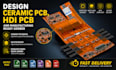
Need a professional Ceramic PCB, HDI PCB, or manufacturing ready Gerber file for your electronics project?
I will design high quality PCB layouts, schematics, and production files using Altium Designer, KiCad, EasyEDA and Cadence OrCAD.
This gig is perfect for ESP32, STM32, IoT hardware, RF microwave circuits, embedded systems, WiFi Bluetooth devices, antenna PCB layout, and compact multilayer boards.
Many buyers face problems like noisy signals, overheating, bad routing, manufacturing errors, poor grounding, and rejected PCB files.
I solve these issues with clean routing, DFM optimization, thermal management, impedance control, and accurate manufacturing ready outputs.
You will receive Gerber files, SCH, BRD, BOM, Pick and Place, PDF schematic and 3D PCB preview ready for JLCPCB, PCBWay, and other manufacturers.
I focus on reliable communication, fast delivery, organized design and professional PCB standards to help startups, engineers, students and businesses build successful hardware products.
Whether you need Ceramic PCB for heat dissipation or HDI PCB for high density compact devices, I will provide a reliable and optimized solution for your project.

Can you provide manufacturing ready Gerber files for PCB fabrication?
Yes. I deliver complete manufacturing ready files including Gerber, BOM, Pick and Place, SCH, BRD, PDF schematic, and 3D PCB files compatible with JLCPCB, PCBWay, Seeed Studio, and other manufacturers to prevent fabrication errors
Can you design HDI PCB, Ceramic PCB, and RF microwave PCB projects?
Yes. I specialize in HDI PCB, Ceramic PCB, RF microwave PCB, antenna layouts, ESP32 boards, STM32 hardware, and multilayer embedded systems with optimized routing, grounding, and thermal management for reliable performance.
What information do you need before starting the PCB design?
You can send your circuit idea, schematic, hand sketch, dimensions, reference files, component list, or project requirements. If you do not have complete files, I can also help organize and optimize the design before PCB development.
Will my PCB design be optimized to avoid noise, heating, and signal problems?
Yes. I use proper PCB design rules, impedance control, grounding techniques, trace optimization, and thermal management to reduce EMI noise, overheating, signal loss, and manufacturing issues in your PCB project.
Can you redesign, review, or improve an existing PCB layout?
Yes. I can review and optimize your existing PCB design for better routing, smaller board size, manufacturing compatibility, improved performance, and error correction before production to help avoid costly mistakes.
