Browse categories
Explore
Fiverr Pro
English
$
USD
PCB Design Engineer
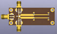
I'm a professional RF PCB Deslgn Engineer delivering high-performance RF PCB design, wireless PCB layout, circuit deslgn, signal integrity analysis, and high frequency PCB solutions for startups, engineers, IoT developers, and electronics manufacturers.
If you're facing signal loss, EMI/EMC issues, impedance mismatch, poor RF performance, unstable wireless communication, or failed prototypes, I provide reliable, manufacturing ready PCB designs that improve performance and reduce development costs.G Every deslgn follows industry best practices for impedance control, trace routing, grounding, power integrity, and RF optimization to ensure dependable operation.
What I Offer
Why Choose Me?
Order now and let's build a high performance RF PCB ready for manufacturing
What do you need to start my RF PCB design project?
Please send your project requirements, circuit diagram, block diagram, specifications, component list, frequency range, and any reference files if available.
Which software do you use for RF PCB design?
I use professional PCB design tools such as Altium Designer, KiCad, EasyEDA, and Eagle CAD based on your project requirements and preferred workflow.
What files will I receive after project completion?
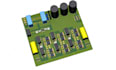
You'll receive schematic files, PCB layout, Gerber files, BOM, Pick and Place files, PDF documentation, and 3D PCB models if required.
Can you design high-frequency and wireless PCBs?
Yes. I design RF PCBs, wireless communication boards, antenna layouts, high-frequency circuits, IoT devices, and impedance-controlled multilayer PCBs.
Will my PCB be ready for manufacturing?
Absolutely. Every PCB is designed according to industry standards and is ready for fabrication by manufacturers such as JLCPCB, PCBWay, Seeed Studio, and OSH Park.
Can you improve or redesign my existing RF PCB?
Yes. I can optimise RF layouts, improve signal integrity, reduce EMI/EMC issues, enhance impedance matching, and redesign existing PCBs for better performance.
Why should I choose your service?
I deliver accurate RF PCB layouts, reliable circuit designs, excellent signal integrity, manufacturing-ready files, fast communication, and professional engineering solutions that help ensure stable, high-performance electronic products.


