I will design custom pcb layout or iot hardware

Poland

I speak English, Polish

Electronic Engineer

I am an Electronics & IoT Prototyping Engineer specializing in custom schematic capture and PCB layout exclusively using KiCad and EasyEDA. I offer end-to-end IoT hardware development, meaning I can t...
About this Gig

Turn Your IoT Concept Into a Functional Physical Prototype!


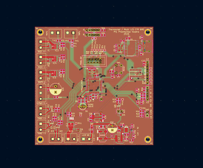
Are you looking for a professional engineer to design a custom PCB layout or build a complete IoT device from scratch? You are in the right place! I specialize in hardware development and rapid prototyping, taking your ideas from a basic block diagram to a ready-to-manufacture electronic product.

️ What I Offer in this Gig:

  • Schematic Capture & Circuit Design: Proper component selection, power optimization, and circuit simulation.
  • PCB Layout (KiCad & EasyEDA): Multi-layer high-density routing, signal integrity management, and optimal grounding.
  • Firmware Development: Robust C/C++ programming for ESP32 (Wi-Fi/BLE), STM32, Atmega, and Microchip MCUs.
  • 3D Enclosure Design: Custom CAD modeling (STEP/STL files) optimized for FDM 3D printing to fit your electronic hardware perfectly.

Deliverables You Will Receive:

  • Complete KiCad or EasyEDA project source files
  • Production-ready Gerber files, NC Drill, and Pick-and-Place data
  • Bill of Materials (BOM) with live component sourcing links
  • High-quality 3D renderings of your board

PLEASE NOTE: Every electronics project is unique. Please contact me via inbox before placing an order.

Specialization:

Circuit design

Schematics

Layout

Footprint

File format:

Gerber

STEP

VRML

BRD

SCH

Software:

EasyEDA

KiCad

LabVIEW

Matlab

Simulink

SolidWorks

Interface:

HDMI

MIPI DSI/CSI

I2S

TDM

UART

USB

SPI

I2C

SDIO

PCIe

Wi-Fi

BT