Browse categories
Explore
Fiverr Pro
English
$
USD
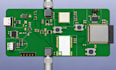
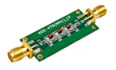
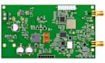
Need a professional RF wireless PCB deslgned for reliable performance and manufacturing? I will deslgn RF PCB layouts, wireless circuits, antenna layouts, impedance-controlled routing, and fabrication-ready Gerber files using KiCad.
My service is suitable for ESP32, Wi-Fi, Bluetooth, BLE, IoT, embedded wireless devices, RF modules, and custom electronic products. I focus on clean PCB layout, proper component placement, controlled impedance routing, RF signal integrity, grounding, power distribution, and design-for-manufacturing practices.
What I can provide:
Whether you need a compact wireless PCB, RF module integration, or a production-ready board, I can turn your requirements into a professional KiCad PCB deslgn.
Please contact me before ordering so we can discuss your project requirements, board specifications, and deliverables.
1. What information do you need to start the PCB design?
I need your schematic, circuit requirements, component list, board dimensions, layer requirements, and any existing design files.
2. Can you design RF and wireless PCB layouts in KiCad?
Yes. I can create professional RF and wireless PCB layouts in KiCad, including component placement, routing, grounding, and manufacturing files.
3. Do you provide antenna design and layout?
Yes. I can design and integrate PCB antennas according to your wireless application, board constraints, and required frequency.
4. Can you handle impedance-controlled PCB routing?
Yes. I can implement controlled-impedance routing based on your stackup, trace requirements, and RF/high-speed signal specifications.
5. Can you design multilayer RF PCBs?
Yes. I can work on 2-layer, 4-layer, and higher-layer PCB designs depending on the project requirements.
6. Do you provide Gerber files for manufacturing?
Yes. I can provide fabrication-ready Gerber files along with the required manufacturing documentation.
7. Can you design PCBs for ESP32, Wi-Fi, Bluetooth, and BLE?
Yes. I can design wireless PCB layouts for ESP32, Wi-Fi, Bluetooth, BLE, IoT, and similar RF applications.
8. Do you provide the KiCad source files?
Yes. The editable KiCad project files can be included according to the selected package.
9. Can you review or modify an existing PCB design?
Yes. I can review existing KiCad PCB designs, identify layout issues, and make requested modifications or improvements.
10. Should I contact you before placing an order?
Yes. Please contact me first with your project requirements so I can confirm the scope, complexity, deliverables, and appropriate package.


