Browse categories
Explore
Fiverr Pro
English
$
USD
Need a professional PCB deslgner for rigid-flex, RF, multilayer, or flexible circuit projects? I can help turn your schematic, concept, or requirements into a reliable, manufacturing-ready PCB deslgn.
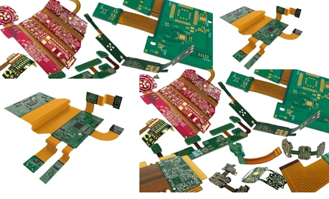
I specialize in rigid-flex PCB, RF PCB, multilayer PCB, flexible circuit, antenna layout, high-speed routing, component placement, and Gerber file preparation. I can deslgn compact and organized layouts with careful routing, proper layer stackup, grounding, power distribution, impedance-controlled traces, and deslgn-for-manufacturing considerations.
WHAT I CAN PROVIDE:
Whether you need a prototype, product development board, wearable electronics, wireless device, or custom circuit layout, I will deliver clean, accurate, and production-ready files tailored to your requirements.
Message me before ordering to discuss your project Requirement.
1. What PCB design services do you offer?
I offer rigid-flex, RF, multilayer, flexible circuit, antenna layout, high-speed routing, and Gerber file design.
2. Can you design RF and antenna circuits?
Yes. I can create RF layouts, antenna placement, controlled routing, grounding, and high-frequency PCB layouts.
3. Do you design multilayer PCBs?
Yes. I can design multilayer boards with suitable layer stackups, component placement, routing, power, and ground planes.
4. Can you work with flexible and rigid-flex PCBs?
Yes. I can design flexible and rigid-flex layouts while considering bend areas, component placement, routing, and board constraints.
5. Can you generate manufacturing-ready Gerber files?
Yes. I can provide Gerber, drill, and other required manufacturing files based on your project requirements.
6. What files do you need to start the project?
Please provide your schematic, circuit files, component information, board dimensions, layer requirements, and manufacturer specifications when available.
7. Can you work from an existing PCB design?
Yes. I can modify, optimize, reroute, or improve an existing PCB layout according to your requirements.
8. Do you provide schematic-to-PCB conversion?
Yes. I can convert your schematic into a structured PCB layout with component placement and professional routing.
9. Can you design compact PCB layouts?
Yes. I can optimize component placement and routing for compact electronics, wireless devices, wearables, and embedded systems.
10. Should I contact you before placing an order?
Yes. Please contact me with your project details and files first so the scope, requirements, and deliverables can be confirmed.
