Browse categories
Explore
Fiverr Pro
English
$
USD
Reliable PCB and Embedded System Design for Real World Applications
High-Speed PCB Design Signal Integrity, Impedance Control, Production-Ready
High-speed designs don't fail because of the circuit, they fail because of the layout. At high frequencies, poor routing, uncontrolled impedance, or mismatched differential pairs can cause signal loss, noise, and complete system failure.
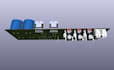
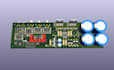
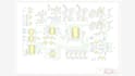
I design high-speed PCBs focused on real signal behavior. This includes controlled impedance routing, differential pair matching, proper stack-up, and clean grounding for stable performance.
️What I Offer
Deliverables
Supported Interfaces
Why Choose Me
Use Cases
Message me before ordering for review.....
File format:
Gerber
•
BRD
•
SCH
•
•
ODB
Software:
Altium Designer
•
Cadence OrCAD
•
EasyEDA
•
KiCad
•
LTspice
Interface:
HDMI
•
MIPI DSI/CSI
•
USB
•
SPI
•
I2C
•
PCIe
•
Ethernet
What do you need to start a high-speed PCB design?
I need your interface details (USB, HDMI, PCIe, etc.), layer requirements, constraints, and any existing schematics or guidelines.
Do you design with controlled impedance?
Yes. I design with impedance control based on stack-up, trace geometry, and manufacturer specifications.
Can you handle differential pair routing and length matching?
Yes. I ensure proper differential routing, spacing, and length matching for signal integrity.
Do you consider signal integrity in your designs?
Yes. I apply proper routing, return paths, grounding, and layout practices to maintain signal quality.
Will the PCB be ready for manufacturing?
Yes. You will receive Gerber, ODB++, and all required files for fabrication and assembly.
Can you review or fix an existing high-speed PCB design?
Yes. I can analyze routing, impedance, and layout issues and optimize your design.
Should I contact you before placing an order?
Yes. High-speed designs require clear specifications, so message me first to ensure proper execution.


