Browse categories
Explore
Fiverr Pro
English
$
USD
PCB Designer l ESP32 Board Designer l Custom Electronics l Circuit Design
Level 1
Has met certain performance criteria and shows strong potential in the marketplace.
Highly Responsive
Known for exceptionally quick replies
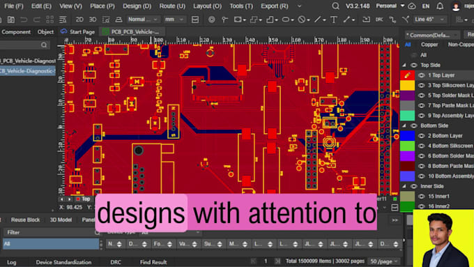
I will design your PCB schematic and layout using KiCad or
EasyEDA professional, manufacturing-ready, and DRC-verified.
What I offer:
- PCB schematic design
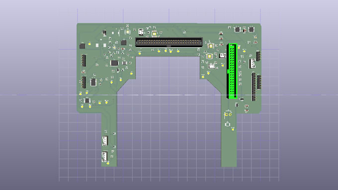
- PCB layout and routing
- Component placement & custom footprint creation
- 2-layer, 4-layer & multilayer PCB design
- ERC/DRC checking
- Gerber & fabrication files
- BOM and component selection
- 3D PCB model
- Manufacturing-ready source files
Interfaces I work with:
USB, UART, SPI, I2C, CAN, Ethernet, HDMI, MIPI
️ Software: KiCad & EasyEDA
I focus on clean layouts, proper grounding, design-rule
compliance, and reliable routing built for real-world
manufacturing, not just simulation.
For complex or custom projects, message me first so I can
understand your requirements and give you an accurate scope.

1. Do you design PCBs using KiCad and EasyEDA?
Yes, I design professional PCBs using both KiCad and EasyEDA.
2. Do you provide the schematic and source files?
Yes, I can provide schematic, PCB source files, Gerber, BOM, and other required files according to the package.
3. Can you design 2-layer and multilayer PCBs?
Yes, I can design 2-layer, 4-layer, and multilayer PCBs depending on project requirements.
4. Do you provide manufacturing-ready Gerber files?
Yes, I provide fabrication-ready Gerber files after completing ERC/DRC checks.