Browse categories
Explore
Fiverr Pro
English
$
USD
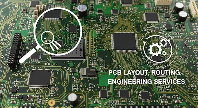
PCB DESIGN AND FIRMWARE DEVELOPMENT
Hello Buyer's welcome to my gig,
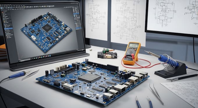
Need a professional PCB de sign for your electronics project? I specialize in PCB layout, PCB routing, PCB engineering, and schematic design, delivering high-quality, production-ready solutions for prototypes and full production.
I offer complete PCB services for hobbyists, makers, startups, and engineers
What I Offer;
Why Choose Me
Ready to de sign your PCB? Click ORDER NOW and get professional PCB layout, routing, and engineering services today!


Can you optimize PCB layout and routing?
Yes, I ensure your PCB layout is compact, low-noise, and ready for manufacturing.
Do you provide prototype-ready files?
Absolutely. All designs include Gerber files and BOM.
Can you create PCB schematics?
Yes, I provide professional schematic capture and circuit design.