Browse categories
Explore
Fiverr Pro
English
$
USD
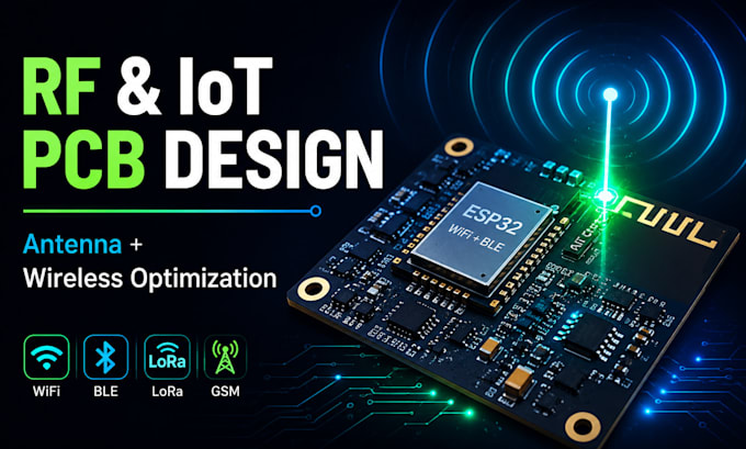
Wireless and RF PCB design requires more than layoutit demands proper antenna integration, impedance matching, EMI/EMC reduction, and signal integrity optimization to ensure stable real-world performance. I will design or fix your IoT/RF PCB with optimized wireless communication and manufacturing-ready files.
Whether you're building IoT devices, smart sensors, wearables, or wireless communication systems, I will ensure your PCB delivers reliable connectivity and clean signal performance.
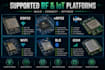
Services include RF & IoT PCB design, antenna integration, WiFi/BLE/LoRa/GSM/LTE optimization, schematic design, PCB layout (28 layers), EMI/EMC reduction, impedance matching, BOM, Gerber files, and optional 3D modeling. Supported platforms include ESP32, nRF52, STM32, LoRa, GSM, LTE, WiFi, and Bluetooth systems.
Please message before ordering to discuss your project requirements and ensure the best results.
Specialization:
Circuit design
•
Schematics
•
Layout
•
Gerber
File format:
Gerber
•
STEP
•
BRD
•
Software:
Altium Designer
•
Eagle CAD
•
EasyEDA
•
KiCad
Do you design antenna-integrated PCBs?
Yes, I design and optimize PCB antenna layouts for WiFi, BLE, LoRa, and GSM systems.
Can you fix my existing RF PCB issues?
Yes, I can analyze and fix signal loss, EMI noise, impedance mismatch, and wireless instability.
What files will I receive?
You will receive Gerber files, schematic, BOM, and source files ready for manufacturing.
Do you support IoT platforms like ESP32?
Yes, I specialize in ESP32, nRF, STM32, and other IoT wireless systems.
Can you handle complex multi-layer PCB design?
Yes, I design 2 to 8-layer advanced RF and IoT PCBs depending on project needs.