Browse categories
Explore
Fiverr Pro
English
$
USD
Hello Buyer's welcome to my gig,
Are you developing a high-frequency, RF, or wireless product that demands precision, reliability, and manufacturability?
You're in the right place.
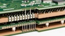
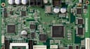
I am a professional PCB design engineer specializing in RF PCB design, HDI layouts, via-in-pad, and controlled impedance routing for modern, compact, and high-speed electronics.
What I Will Do
Tools I Use
Message me before ORDERING to discuss your RF requirements and choose the best package for your project.

Can you work with my PCB manufacturer’s rules?
Yes, I can design strictly according to your manufacturer’s DRC and impedance constraints.
Do you design antennas as well?
Yes, I can route antenna feeds and assist with antenna PCB layouts.
Is this suitable for mass production?
Absolutely. All designs are DFM-checked and production-ready.
Can you sign an NDA?
Yes, confidentiality is fully respected.


