I will do rf pcb design with hdi, blind, buried vias and power integrity optimization

United States

I speak English, Spanish, German

PCB Design Engineer

I am a detail-oriented PCB Design Engineer with experience in schematic capture, multilayer PCB layout, and design for manufacturing (DFM). I am skilled in delivering reliable, cost-effective, and hig...
About this Gig

Hello Buyer's,

High frequency hardware fails fast when layout, power delivery, and RF routing are not engineered together.

That's where I come in.

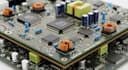
I provide professional RF PCB design services with a strong focus on HDI architecture, blind & buried vias, and power integrity (PI) to ensure stable operation, low noise, and reliable performance in real-world conditions.

What I Offer;

  • RF and mixed-signal PCB layouts
  • HDI boards with blind & buried vias
  • Power distribution networks optimized for low noise
  • Clean RF signal paths with proper return currents
  • Multilayer stack-ups for high-frequency systems
  • Ground isolation, stitching vias, and shielding
  • Low-ripple power planes for sensitive RF blocks
  • Power Integrity Focus
  • Decoupling & bulk capacitor placement strategy
  • Low-impedance PDN design
  • Power plane segmentation & stitching
  • Noise isolation between RF, analog, and digital rails
  • RF Applications
  • Wireless communication boards
  • IoT & industrial RF devices
  • RF sensor electronics

Message me before ORDERING so we can review your RF and power requirements and choose the right approach for your design.


Specialization:

Circuit design

Schematics

Layout

Footprint

File format:

Gerber

STEP

VRML

SCH

PDF

Software:

Allegro

Altium Designer

Eagle CAD

EasyEDA

Fusion 360

Interface:

HDMI

I2S

TDM

UART

USB

SPI

I2C

Wi-Fi

BLE

BT

GSM/GPRS

Ethernet