Browse categories
Explore
Fiverr Pro
English
$
USD
PCB Design , Electronics Hardware Specialist
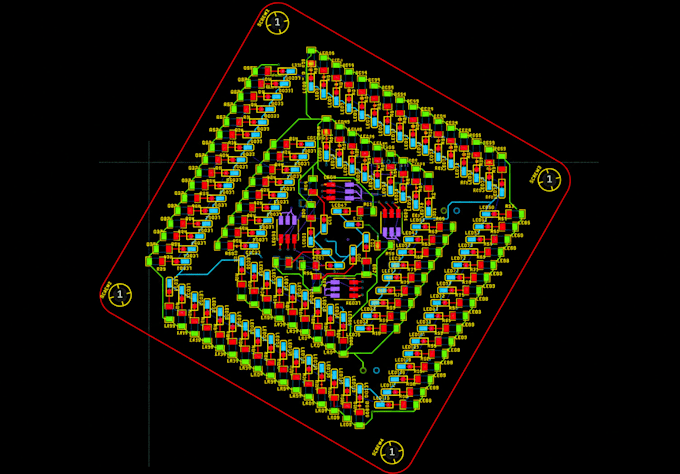
I am an Electronics Hardware Engineer with 7+ years of experience in LED PCB, aluminum PCB, and IMS layout design. I build integrated LED driver boards using Altium Designer with complete 3D STEP BOM deliverables.
Services I Offer:
Tools I Use:
File Formats Delivered:
Why Work With Me?
Please message me to discuss your project requirements before placing a direct order!


What files or specifications are needed to initiate an aluminum PCB layout?
To begin, please send your electrical requirements (voltage, current, power rating), mechanical dimensions (DXF or STEP housing file), and datasheets for selected LEDs or driver ICs.
What is an Insulated Metal Substrate (IMS) and when should I use it?
An IMS board features an aluminum base, a thermally conductive dielectric layer, and a top copper circuit layer. You should use an aluminum PCB when managing high power density LEDs, as it transfers heat away much faster than standard FR4 material.
Can you design the LED driver directly onto the same board as the LEDs?
Yes. I regularly design integrated switch-mode and linear LED driver circuits directly on the main PCB or IMS substrate to create compact, all-in-one lighting modules.
Why is a 3D STEP model included with the Bill of Materials (BOM)?
The 3D STEP model allows mechanical engineers to verify component height clearances and connector alignments inside your housing CAD model before manufacturing, while the BOM ensures exact component purchasing.
Which design software do you use for schematic capture and layout?
I complete all schematic designs and board layouts in Altium Designer. This ensures precise clearance checks, native 3D STEP exports, and clean production outputs.
How do you address thermal dissipation on high-power LED boards?
I use copper pour areas, strategic thermal via placement, precise trace widths, and optimized component placement to spread heat evenly across the aluminum substrate and prevent junction overheating.