Browse categories
Explore
Fiverr Pro
English
$
USD
Student at Institut National des Postes et Telecommunications
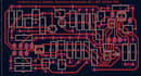
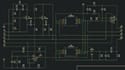
Are you looking to transform your circuit idea, prototype, or schematic into a professional, manufacturing-ready PCB layout? You've come to the right place!
I specialize in custom PCB design, schematic capture, and circuit optimization for embedded systems, IoT devices, and general electronics projects.
What I Offer:
Software Expertise:
Whether you need a quick 2-layer sensor board or a complete multi-layer hardware solution, I deliver clean, industry-standard design outputs ready for fabrication (JLCPCB, PCBWay, etc.).
Please message me before placing an order to discuss your project requirements, target dimensions, and component availability!

File format:
Gerber
•
STEP
•
BRD
•
SCH
•
Software:
Cadence OrCAD
•
KiCad
•
Proteus
•
PSpice
Interface:
UART
•
USB
•
SPI
•
I2C
•
Controller Area Network (CAN)
What software do you use for PCB design?
My primary workflow is KiCad, but I can also accommodate projects using Proteus or ORcad depending on your preferences.
What manufacturing files will I receive?
You will receive industry-standard Gerber files (RS-274X), NC Drill files, Pick & Place (CPL) files, a detailed BOM (Bill of Materials), PDF schematics, and source files.
Can you provide a 3D model of the finished PCB?
Yes! I can export 3D STEP models of the PCB assembly, which you can import into Fusion 360, SolidWorks, or other CAD tools for custom enclosure fitting.
What do I need to provide before starting the order?
Please share a clear schematic sketch, block diagram, list of key components/connectors, and any mechanical constraints (board dimensions, mounting holes, etc.).


