Hello Everyone
Welcome here.
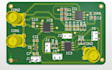
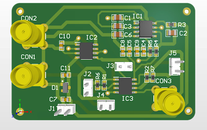
As an Electronic Engineer, I will design Professional PCBs for your projects and industrial use.
I am working as a PCB Design Engineer at R&D Altanova Advantest.
JOB DESCRIPTION:
- Component development and library management.
- Created schematic symbols and layout footprints.
- Good understanding of reading engineering drawings and layout/footprint of complexed components.
- high-speed, controlled impedance boards with RF and mixed signals routing
- Formulated all kinds of reports including BOM, Net-list, Net-length Assembly reports
- Collaborated with the team on several projects to complete within a strict time-frame.
- Design diverse PCB test boards on various ATE platforms for leading chip manufacturers including NXP, NVIDIA, AMD, INTEL, HISILICON, LATTICE, BROADCOM, XILINX etc.
My service will include:
- Gerber files for fabrication.
- Schematic file with no extra charge. (when circuit diagram is given)
- BOM (Bill of material)
- Source file of Altium Designer
- PCB of your desired shape
- Impedance controlled routing taking care of IEEE standards for high-frequency designs.
- Design in through hole and SMD.