Browse categories
Explore
Fiverr Pro
English
$
USD
Electronics Engineer
Looking for professional PCB routing and layout design?
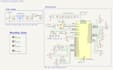
I will design clean, organized, and efficient PCB layouts for your electronic projects. My services include PCB track routing, component placement, schematic-to-PCB conversion, layout optimization, and Design Rule Check (DRC) error correction.
My Services:
Software: KiCad, Proteus and EasyEDA.
I focus on accurate routing, proper component placement, and reliable PCB layouts according to your project requirements.


What information do you need to start my PCB design?
I need your circuit schematic, project requirements, preferred board dimensions, component details, and any specific design constraints.
Which software do you use for PCB routing and layout design?
I use KiCad ,proteus and EasyEDA to create organized PCB layouts and route tracks according to your project requirements.
Can you convert my schematic into a PCB layout?
Yes, I can convert your provided electronic schematic into a PCB layout, including component placement and track routing.
Can you work with an existing PCB design?
Yes, I can review an existing PCB design and make agreed modifications, routing improvements, or layout corrections based on your requirements.


