Browse categories
Explore
Fiverr Pro
English
$
USD
PCB Design Engineer, Altium Designer
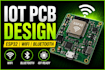
IoT PCB Design in Altium | ESP32, Wi-Fi, Bluetooth
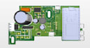
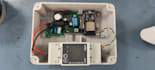
I am an Electronics Engineer specializing in IoT PCB design, schematic development, and wireless circuits. I create high-quality, manufacturing-ready PCB designs using Altium with proper layout practices for stable and reliable performance.
️ Services I Offer
IoT Expertise
Why Choose Me?
️ Note: Pricing depends on project complexity. Please message me to discuss your requirements before placing an order.
File format:
Gerber
•
STEP
•
SCH
•
•
ODB
Software:
Altium Designer
•
EasyEDA
•
KiCad
•
LTspice
•
Proteus
Interface:
UART
•
USB
•
SPI
•
I2C
•
Wi-Fi
•
Controller Area Network (CAN)
What do you need to start the PCB design?
I need your circuit idea, reference schematic (if available), dimensions, and component details.
What files will I receive?
You will get Gerber files, PCB layout, schematic (if selected), BOM, and source files (Altium/KiCad).
Can you design multilayer PCBs?
Yes, I can design Multi-layer PCBs based on your project requirements.
Do you provide fabrication-ready files?
Yes, all designs include manufacturing-ready Gerber files.
Do you offer revisions?
Yes, revisions are included based on the selected package.


