Browse categories
Explore
Fiverr Pro
English
$
USD
AI Image Editor , Electrical Engineer , LinkedIn Profiles and Technical Writer
Are you a startup or maker struggling to turn your idea into a PCB design that actually works?
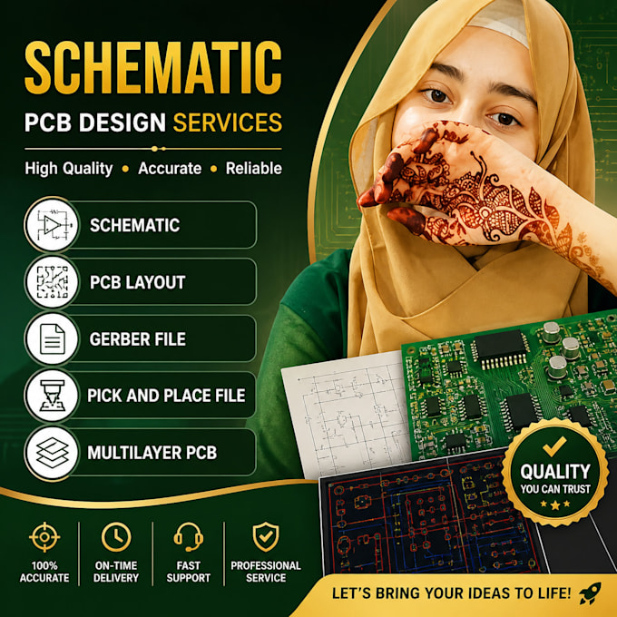
I specialize in IoT PCB design from schematic capture to fab-ready Gerber files for smart home devices, wearable electronics, BLE beacons, and ESP32 PCB and nRF52-based prototypes. Whether you are a first-time hardware founder or an engineer who needs extra bandwidth, I deliver clean, manufacturable boards fast.
What you get:
Schematic design in KiCad, EasyEDA, or Proteus
2-layer or 4-layer PCB layout with DFM best practices
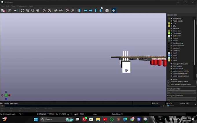
3D STEP model for mechanical and enclosure fit check
BOM optimization with LCSC part numbers cuts cost 1030%
Gerber files + drill files in a fab-ready ZIP
CPL placement file for JLCPCB SMT assembly
My IoT expertise:
ESP32 · ESP8266 · nRF52840 · STM32 · RP2040 · Arduino
Wi-Fi · Bluetooth LE · LoRa · USB · I2C · SPI · UART
Why clients choose me:
IoT-first approach: antenna keep-out, impedance matching, power decoupling done right
BOM optimization saves real money on your first production run
Proteus simulation available test your circuit before ordering boards
Message me before ordering. I review every brief before we


What software do you use, and will I be able to edit the files?
I work in KiCad (free and open source — you can edit it without buying any software), EasyEDA (browser-based, no install needed), and Proteus. Every order includes the native source file for the tool you choose, so you can open and modify the design at any time. Universal Gerber files are also inclu
Are the files ready to order from JLCPCB or PCBWay straight away?
Yes. Standard and Premium packages include a Gerber ZIP, a BOM with LCSC part numbers, and a Component Placement List (CPL) — all formatted for JLCPCB one-click ordering including their SMT assembly service. You can upload the ZIP directly to JLCPCB and place an order without any extra work
What information do I need to provide before you start?
To get started I need: (1) a description of your device and what it does, (2) the microcontroller or main IC you want to use — for example ESP32, nRF52840, or STM32, (3) your power source (USB, LiPo, coin cell), (4) any size or form-factor constraints, and (5) any reference circuits, datasheets, or