Browse categories
Explore
Fiverr Pro
English
$
USD
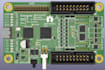
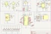
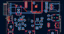
I am an electronics engineer specializing in embedded hardware and PCB design. I will design complete, production-ready PCB schematics, generate accurate BOM and Gerber files using KiCad.
What you get:
My background includes medical grade hardware design and custom IoT devices with complex power management, SPI, I2S, and ADC interfacing.
Specialization:
Circuit design
•
Schematics
•
Layout
•
Footprint
•
Gerber
File format:
Gerber
•
BRD
•
SCH
•
Software:
EasyEDA
•
KiCad
•
Matlab
•
NI Multisim
•
Arduino
Interface:
HDMI
•
I2S
•
UART
•
USB
•
SPI
•
I2C
•
Wi-Fi
•
BLE
•
BT
•
Ethernet


